Electronics researchers have developed a new way to stack transistors in a die, to keep Moore’s law alive for as long as possible

For 60 years, Gordon Moore’s observation that transistor counts in integrated circuits would double roughly every two years has been spookily accurate. Ever-smaller transistors and ever-larger chips have made this possible, but with the physical limits of both impacting the growth of computing, new methods are required to continue the growth. One semiconductor research team claims to have achieved just that by stacking not chips or dies, but individual transistors.
The work by the team at King Abdullah University of Science and Technology (KAUST) in Saudi Arabia was published in Nature Electronics (via El País), and as is always the case for such academic research, it’s all very complicated. Basically, though, it comes down to the idea that chip makers are looking to go up, rather than using smaller transistors or wider dies, to keep Moore’s ‘law’ alive.
Processors such as AMD’s Ryzen 7 9800X3D utilise hybrid bonding techniques to stack dies on top of each other, to increase the number of transistors in the whole package, so there’s more cache. All SSDs today rely on multi-layer NAND flash memory to improve capacity, performance, and reliability.
However, none of these methods fundamentally change the fact that the very best CPUs and GPUs are all fabricated in such a way that there is only one layer of transistors in each chip. This is where the research work at KAUST comes in, because the team managed to create a stack of up to six alternating transistors and used them to make inverters and gates.
The whole thing comprises 41 layers of metals, organic materials, and semiconductors; that’s more layers than you’d find in total for a complete processor. Just making a single stack of two transistors is a serious challenge, though, as the smoothness and alignment of each layer need to be extremely fine.
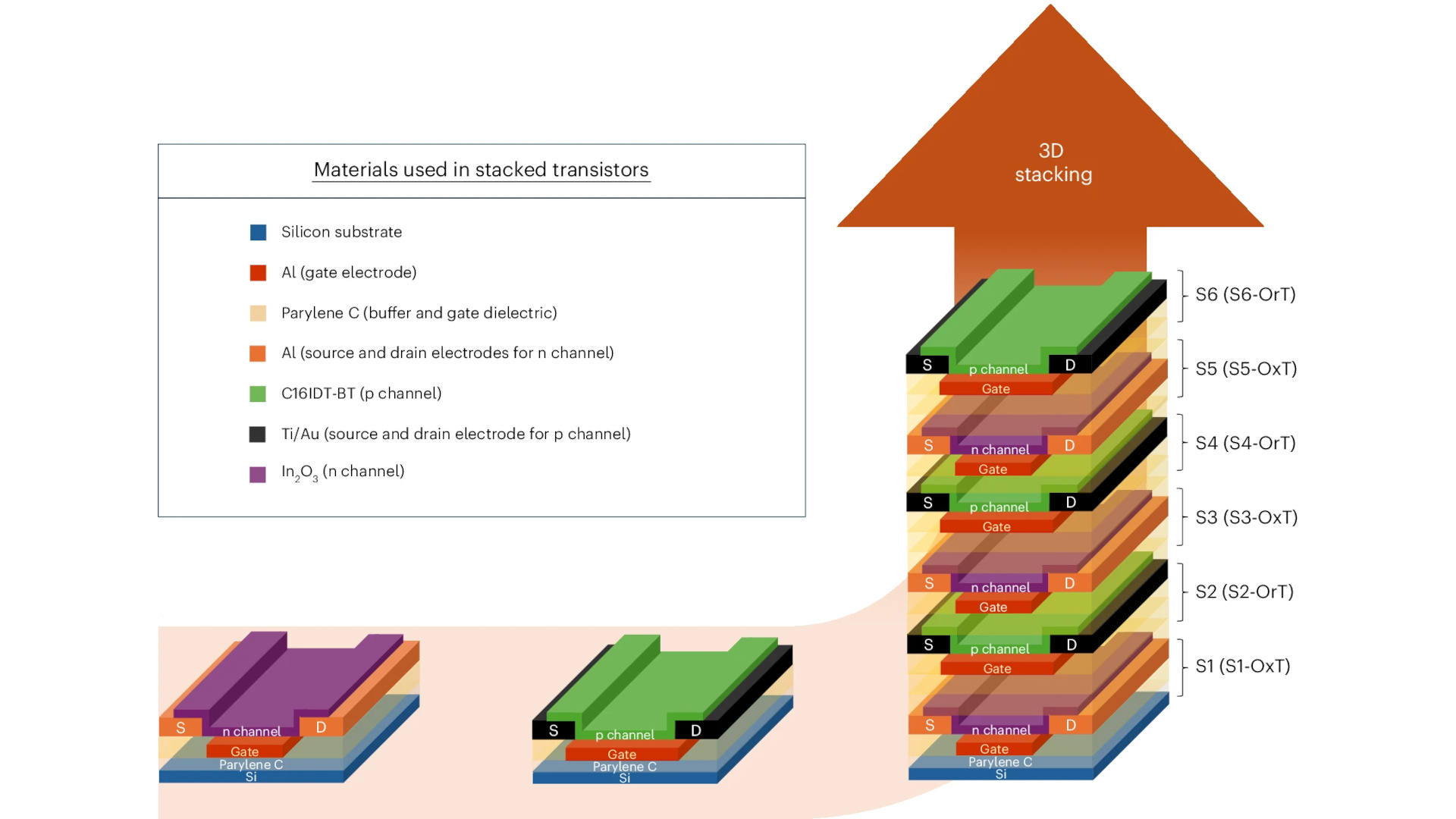
Even just a handful of nanometres here and there can potentially lead to a significant drop in performance. KAUST’s team managed to achieve a surface roughness of no more than 3.63 nm, which is why this work is so significant.
It should be noted that the types of transistors being used aren’t the kind that are perfect for high-power, high clock speed applications, such as big CPUs and GPUs. The six-deep stack of metal oxide and organic thin film transistors developed here has quite a low thermal limit (just 50 °C, with notable instability at 75 °C), but it’s fine for situations where power levels are very low, such as wearable tech or Internet of Things (IoT) devices.
While the manufacturing techniques employed to develop the six-transistor stack are very much ‘laboratory-based’, all mainstream chip production methods started life this way. If the thermal robustness of the stacks can be improved and the fabrication scaled to a suitable level and cost-effectiveness, we’re likely to see this being employed to make the chips of the future.
Moore’s ‘law’ came about because transistors were being made smaller and smaller, every few years, allowing for more to be packed into the same amount of space. Eventually, the likes of Intel, TSMC, and Samsung won’t be able to shrink them any more, but by then, they’ll probably be stacking them sky-high instead.